
In this post, we will be discussing how to use an IP from the IP catalog to make it functional in your custom code using XILINX Vivado.
-
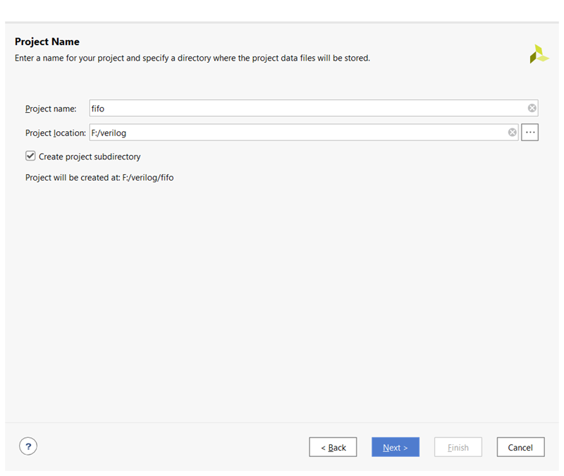
Open Xilinx Vivado and click on create project.

-
Name the project ‘FIFO’ or according to your preference and keep clicking the next tab.
-
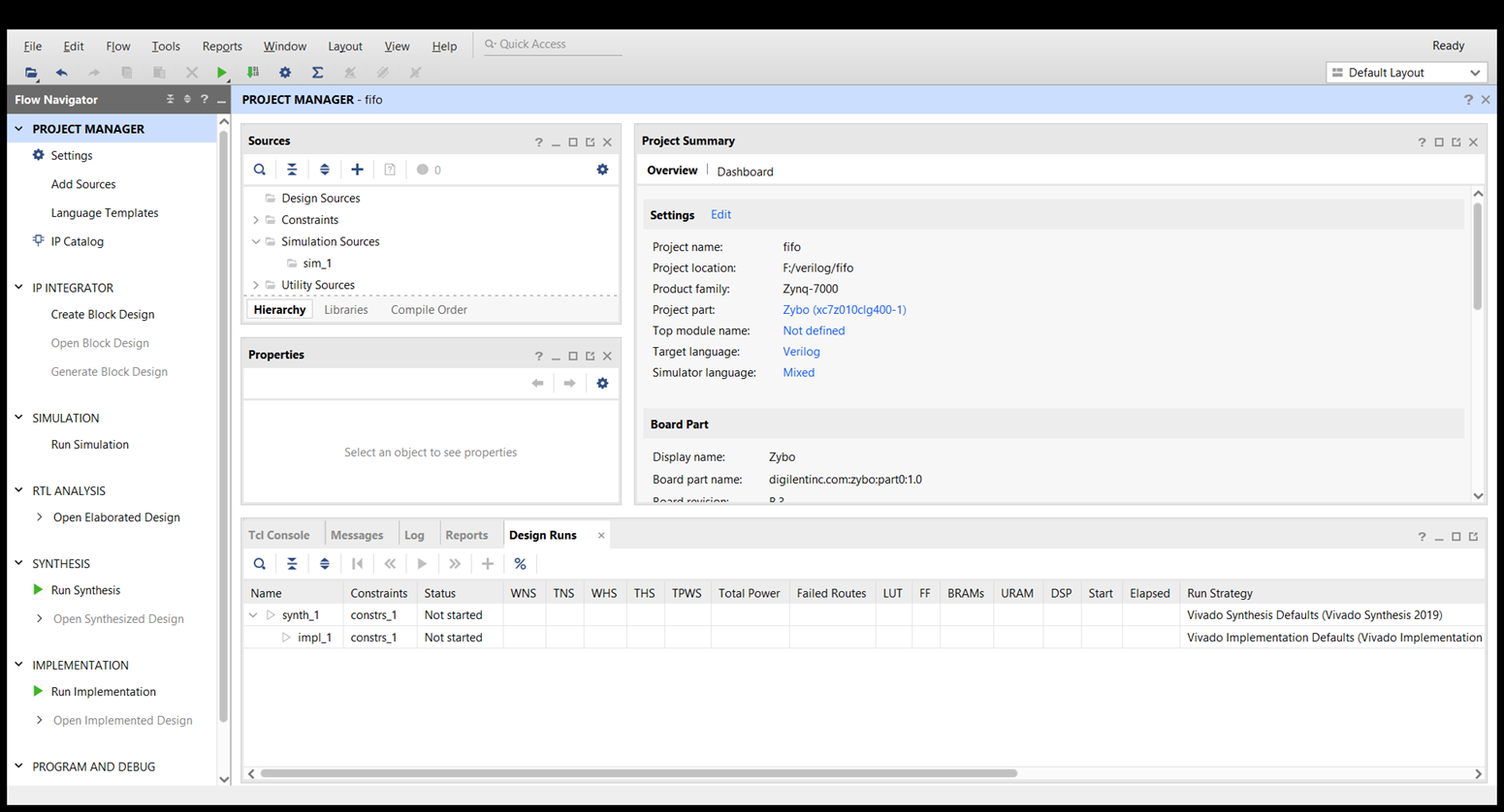
Specify the FPGA board which you have currently in use. Then click on finish. You will see the dashboard as shown in the image below.
-
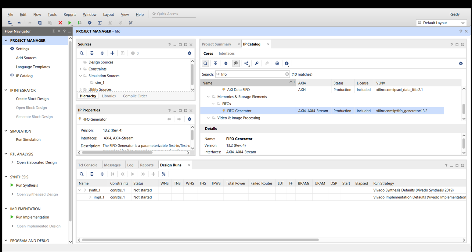
Click on the IP catalog and search ‘fifo’ in the search bar. You will see different IPs provided by Xilinx for use in your design. Double Click on the FIFO Generator (If one more window appears then click on customize IP).
-
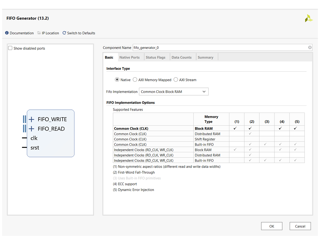
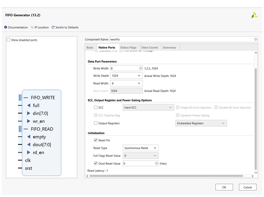
A window will appear where you can customize your FIFO according to your requirement such as changing the size, depth, and interface of your FIFO. The FIFO can be customized in the following ways
- Interface type- there are mainly three types of interface provided by Xilinx for FIFO generator IP those are native, AXI memory Mapped, for basic design of the FIFO native interface is suitable whereas when going for high-performance architectures AXI interface comes in handy.
- FFIO implementation can be altered by selecting different methods such as common clock, independent clock. This field defines how your FIFO will be implemented in your FPGA. It can either be a block RAM with a single clock or built-in FIFO with independent clocks.
- Native ports involve different ports such as input/output range and address depth.
- The status flag contains all the different flags which help in the identification of the data storage in the IP such as almost full, almost half, Full, empty.
- Data count will create an output port for the specified amount of data.
- So, let’s customize our FIFO IP to be used in our custom code. Rename the IP to a simple term like ‘newfifo’ and change the I/O range to 8-bit (we can go for any range specified by the FIFO Generator
-
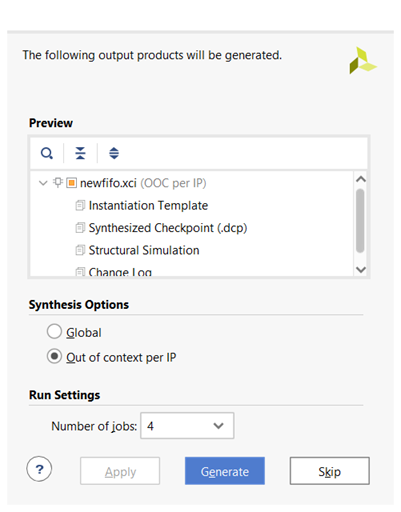
When you expand the FIFO_WRITE and FIFO_READ ports you will see multiple internal ports such as full, din[7:0], and wr_en but these are the signals which help in achieving more control on your IP. When wr_en (write enable) flag is high data can be written to the FIFO and when rd_en (read enable) flag is high data can be accessed from the FIFO. Click ok when you are done customizing the FIFO IP. A window will appear to create a directory so click ok. After that, you will see a window asking to generate the output products so click generate and wait till output products generation is finished.
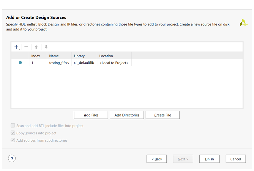
- Create a new source file where we can instantiate our FIFO IP and run it to test the functionality. Click on add source and click on add or create design source. Click on create a file in the next window and name the file as ‘testing_fifo’.
-
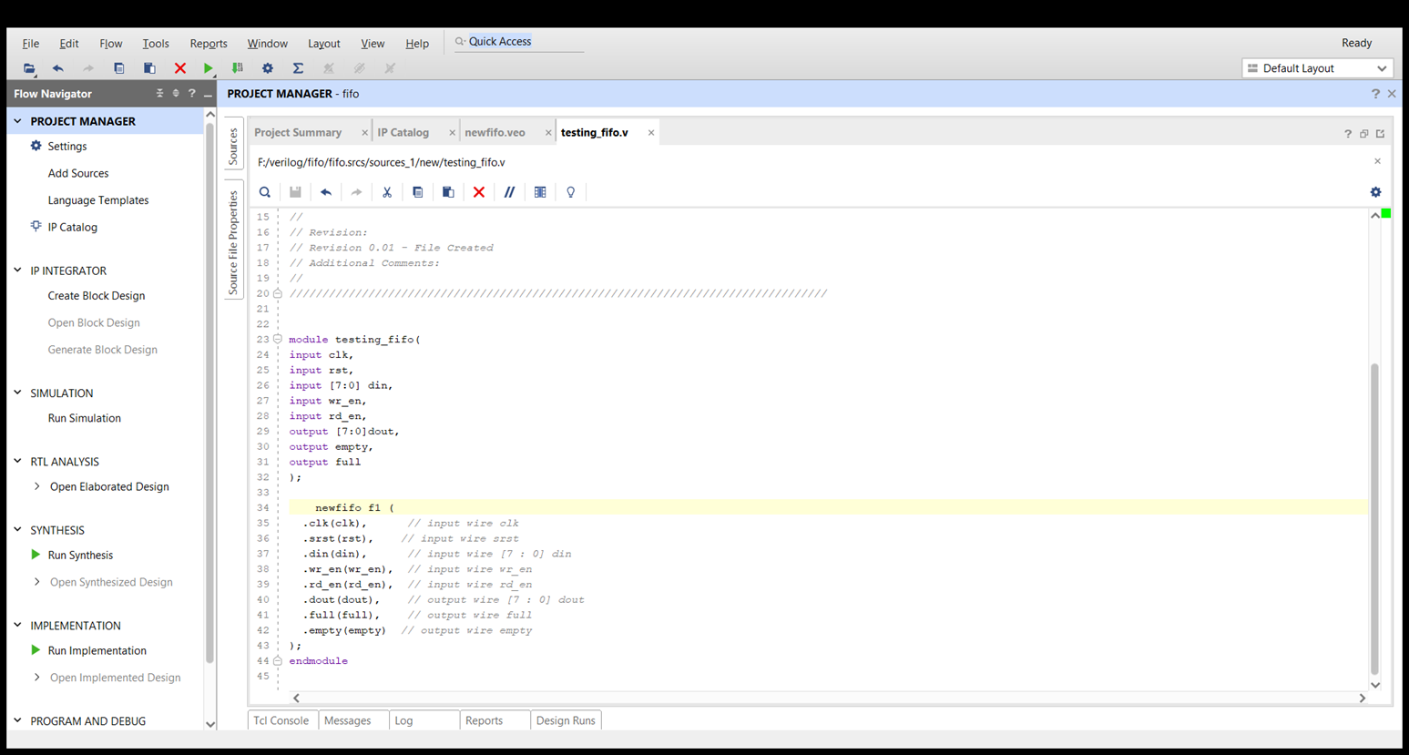
Click on finish and then click on ok when defining module window appears (this window declares the input-output at the initial stage, but we can specify them manually on the file). Double click on testing_fifo.v file and a blank file will appear with only module and endmodule definition.
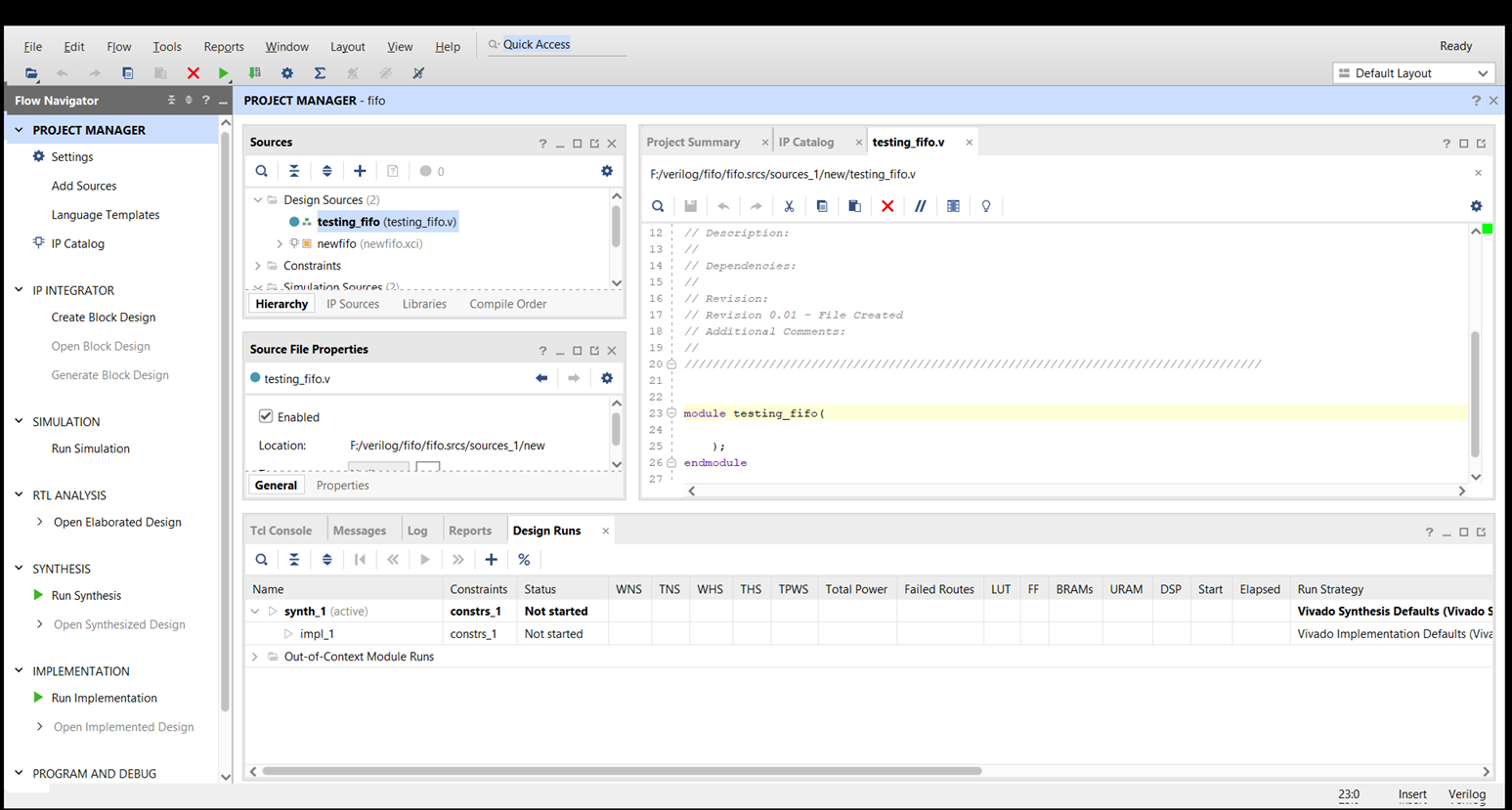
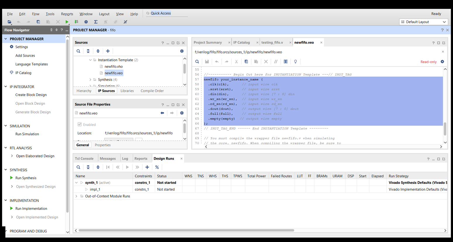
- Click on IP sources next to the Hierarchy tab and click on Instantiation template. In this way, we can instantiate our customized FIFO IP. Then click on newfifo.veo to open the instantiation template. There is two instantiation templates for Verilog as well as Vhdl. If we are going for Verilog language, then .veo extension is used but if Vhdl language is used then .vho extension is used.
-
Copy the content in newfifo.veo and paste it into testing_fifo.v. now we need to specify the input and output for testing our FIFO IP.
-
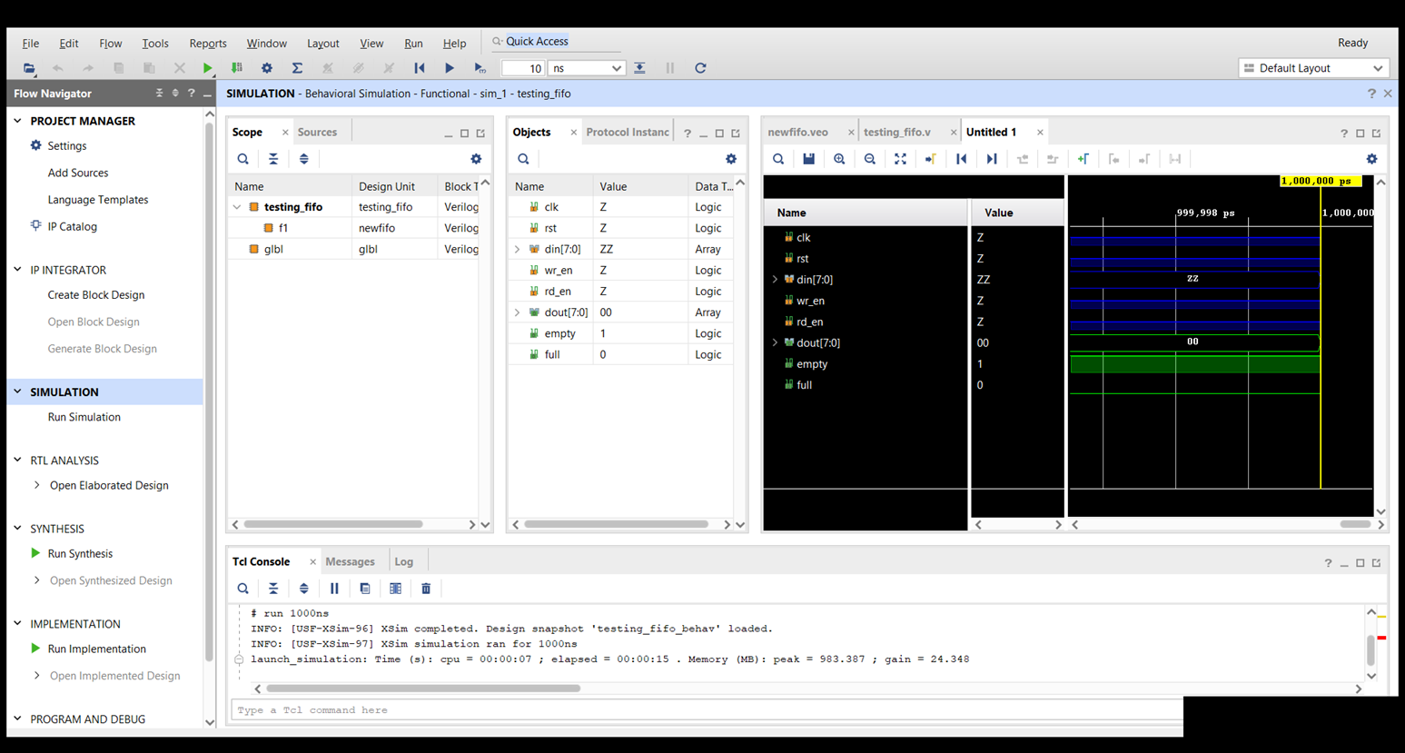
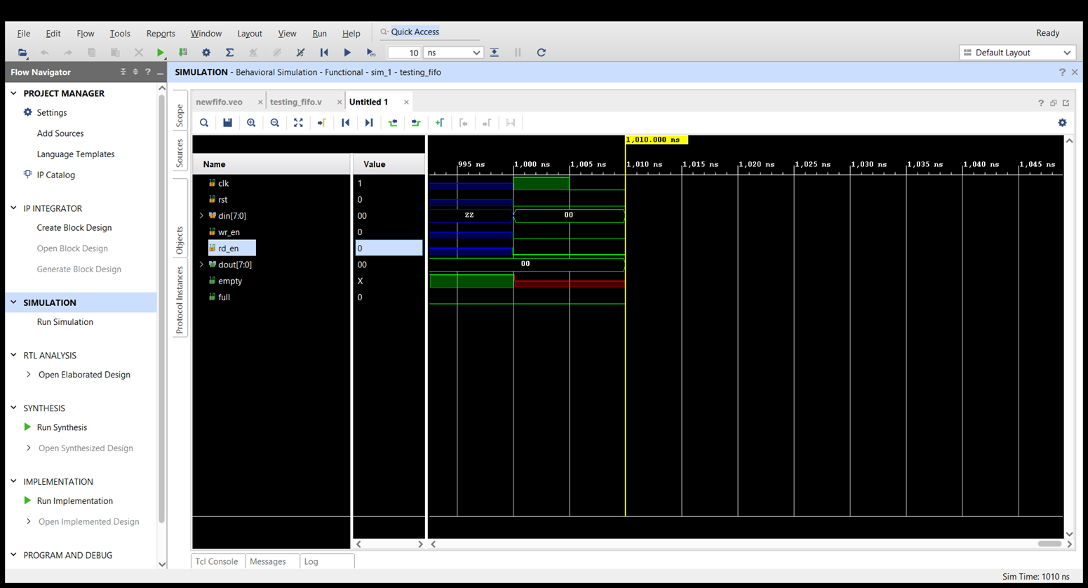
Save the file and click on run simulation for verifying the functionality of the FIFO. A simulation window will appear where signals are marked as ‘z’ or ‘0’. This is due to the absence of input to the design under test (DUT), so there are two ways to simulate our design, which is we can either write a testbench or we can either force our inputs to the simulation window. In this case, we will be forcing input signals to the design then we will be observing the output.
-
Right-click on ‘clk’ and click force clock. Then fill in the entries to make the clock of 10ns period with a duty cycle of 50%

-
Similarly, Click on all the inputs and force constant 0 to each signal.
-
After forcing the inputs with value 0. Click on the play symbol just beneath the help tab and make sure the time period is mentioned as 10ns.

-
This will simulate the FIFO for the next 10ns so that we can see the values incoming to our design.
-
We have provided every input signal as value ‘0’ so now let’s alter some signals in a way that we can store the data to our FIFO and then access it from dout port.
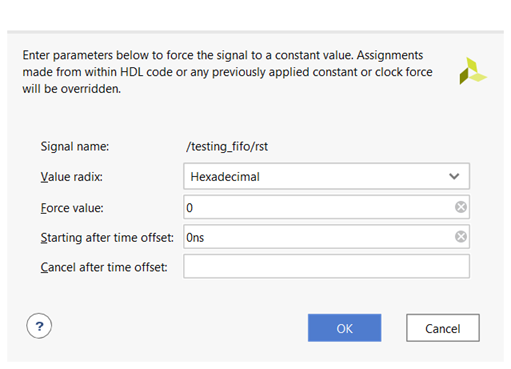
- Force rst to 1 to reset the design and then force it back to zero so that all the internal registers will now hold value zero.
- After reset, Force wr_en to ‘1’ and force some input data to din port.
- Keep the data going for some time then alter the wr_en signal to ‘0’ and rd_en to ‘1’.
-
When rd_en goes high the data stored in the FIFO reflects at the output port dout.
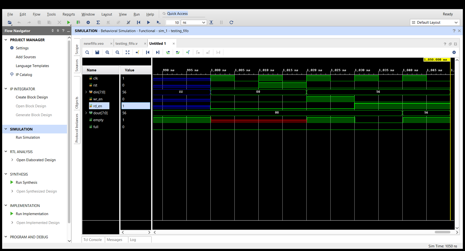
- By simulating the FIFO we saw that our design can store the data and read the data by changing the values of flag registers. Hence the IP can be used in any custom code.
Thanks for reading the post. If you have any queries or suggestions, feel free to contact me.